Galaxia (GalaxyX) Arcade Renovation – Part 1

In a universe far far away live a species closely related to the Galaxians, these ‘people’ were created by the Shoei Corporation for their “Galaxia” clone of the classic game. Some decades later I purchased a completely non-working arcade cocktail table on Ebay for a small-ish sum and here we start the journey to get something working.

My machine is the cocktail sit down version and my own looks a little worse for wear compared to the original (circa 1980 flyer)!

but I’m pretty sure the aliens from GalaxyX are in there somewhere…

Now if that isn’t cool side art I don’t know what is! (And you can even see it in the flyer above so this is the real deal). Now I know many people would consider this just a ‘bootleg’ and the licencing agreement if any between Midway and Shoei is not known I think it’s awesome.

I bought the machine in a non-working state, with no life from the monitor and/or the PCB and a look inside confirms the machine is a bit worse for wear… lots of mildrew type mould and much of the ply looks like it is separating due to decades of storage in a damp environment.

but most of the bits seem to be present including the coin box (locked!), coin mechanism, monitor and PCB etc.

Coinbox
Coin mechanism, step-down transformer, PSU etc

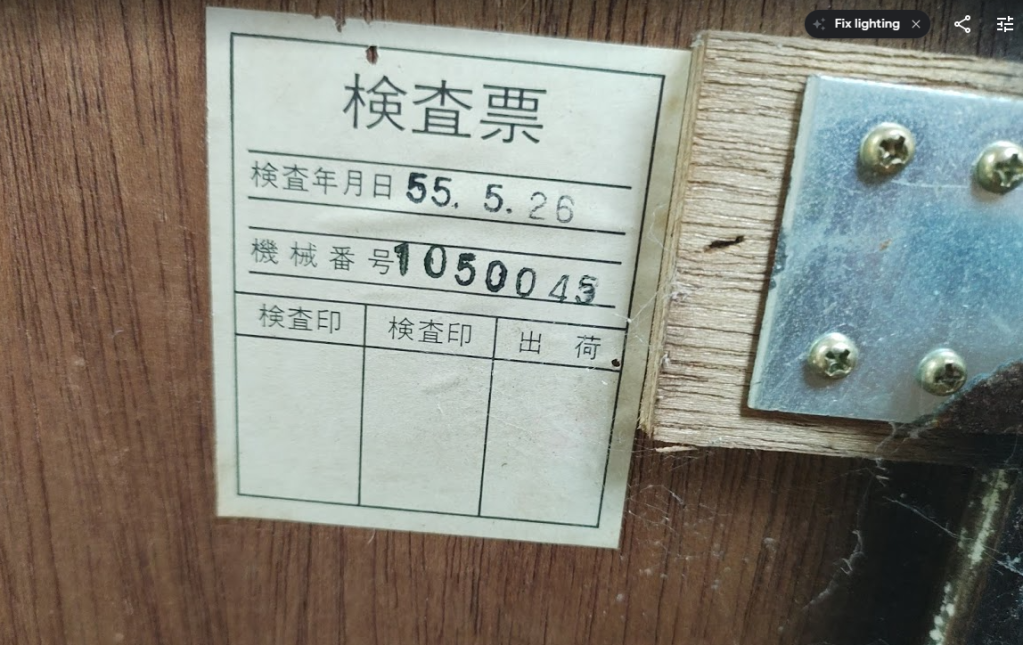
There is a quality control label on the inside…

Showa 55

Now I know from a previous encounter that these Japanese cocktails use the Japanese calendar on their labels so we need to translate Year 55. The years are related to emperors and 55 is “Showa 55” so that dates the table to 1980 in the Western Calendar. 1980… what a year… I was doing my GCSEs… O-Levels… Number ones included “There’s no one quite like Grandma” by the St. Winifred’s School Choir.. we were so cool back then.

A peak at the monitor…

14″ Matshushita Monitor

I really don’t know anything about monitors but it is clear we have some major issues here… when power is applied there is no life at all, the general state looks OK, there are signs of rust on the chassis but no major water damage; the tube itself doesn’t have major burn in. It’s a cute 14″ monitor… a job for another day.

On the other side of the table we see the game PCB angled down into the darkness, attached by two wooden runners, the board itself has a raised daughterboard with some UV EPROMs and generally the whole thing looks pretty crusty.

A peak at the PCB

In further instalments we can look into each of the pieces and see if anything is salvageable.

Posted in Uncategorized | Leave a comment

NuTone LD49N Door Chime – Part 1 – A first look

I am very easily side-tracked and for some time I have been interested in adding chimes to my various radio controlled clocks.  Westminster chimes  or variants thereof are often found in vintage mantel clocks and door chimes and also find enthusiasts in the hobby crowd for whom a micro-controller and some tuned pipes or chimes can develop into an interesting project.  I’ve mused around doing a project for some time and then stumbled across an EBay listing for a broken door chime (a 1950s? V & E Friedland Limited 8 note electric chime), quickly acquired for a low price and now stored safely for some point in the future to investigate further.

In the meantime I decided to do some research into door chimes generally and stumbled across a remarkable YouTube channel by Northside Sevices.  Northside clearly love all things NuTone including door chimes through the generations and the combination of loving owners keeping their vintage stuff alive and perhaps a new demand for retro chic will hopefully keep them very busy.  On their channel I came across a video showing the workings of several chimes across the ages, with early electro-mechanical types to more modern micro controlled solutions but one I found particularly interesting is the LD49N which is a simple design from discrete logic.  Working from the video I have been trying to work out the schematic… well I said I am easily distracted!

Essentially the circuit revolves around a 4017 decade counter. The decade counter has ten states 0,1,2,3,4,5,6,7,8 and 9.  0 is an idle state, 5 in a quiet state and then the solenoids which drive the chimes themselves are mapped to the other numbers.  Despite the name 8-note chime the actual device can only produce 4 different notes, but with each note played twice during the sequence… that gives eight notes.. (someone in marketing must have come up with that one!).

I haven’t completely worked it out but this is what I have so far…

composite2

Each solenoid is connected to a Pin on the board, each solenoid pin is driven by a power transistor (with a Diode to handle reverse EMF when the transistor turns off), the transistor is driven by two states of the decade counter.  I think there is additionally a “Solenoid Inhibit” which turns off the solenoid, presumably to ensure notes don’t run into each other.

So for example, Pin 1 is driven by states 1 and 8.

Pins 2 and 4 have an additional input which is driven by logic for the Side and Rear door inputs.

Drivers
I’m still trying to work out the front end logic but it is all based on a hex Schmidt invert-er chip.  The Front door input enables an oscillator made up of the 2A/2Y and 3A/3Y inverters, the clock for the 4017 being derived from 2Y.  The oscillator will run until state 0 is reached (after state 9 or by a Reset at State 5 if 4-note only is enabled).  The 3Y output seems to drive the solenoid pulse duration.

The Side and Rear door inputs seem to drive chimes attached to Pin 2 and Pin 4.  It looks like the Rear input will cause two chimes to sound, whereas the Side door just drives the chime attached to Pin 2.FrontEndLogic

It’s early days yet and I will probably need some more input from Northside but it would be great if I can fully document this interesting circuit… and after all it keeps me from doing anything useful which is always a good thing!

Posted in Uncategorized | Leave a comment

Solar Eclipse August 21st 2017 – Calculations 1 – Greatest Eclipse

If you haven’t been living in a cave then you should know that in August this year, 2017, something awesome is planned for North America and if you have been living in a cave then you will be very surprised when the world goes dark for the total solar eclipse of August 21st.  Seriously if you are not aware of the magnitude of this event then get googling, go to www.eclipse2017.org or maybe www.space.com or eclipse.gsfc.nasa.gov and get yourself informed and start making your travel plans!

The solar eclipse takes place when the moon passes between the earth and the sun and  due to some very favorable geometry blocks out all (total) sunlight during the transit.  To observe the effect you need to be in the right place at the right time and in the case of the August 2017 eclipse this is along a line that passes across North America.  Only on a very narrow part of the line, the umbral shadow, will the effect be total (and awesome) although in the penumbral  wider zone there will a partial obscuration.  To get the best effect you need to be in the narrow strip of totality.

Predicting the eclipse requires knowledge of the motions of the sun, moon and earth but fortunately the hard work has been done by eclipse experts and is publicly available from sources such as Fred Espenak and it is Fred’s calculations that form the basis of the rest of this post.  The calculated eclipse elements are published here https://eclipse.gsfc.nasa.gov/SEbeselm/SEbeselm2001/SE2017Aug21Tbeselm.html are referenced here and acknowledged “Eclipse Predictions by Fred Espenak, NASA’s GSFC”.  Thanks!

An eclipse can be described in many ways but thanks to the work of Bessel and later  Chauvenet, a scheme was devised to characterize an eclipse by describing the shadow axis between sun, moon and earth. The Besselian elements, themselves described as a series of time dependent polynomials, can then be evaluated during the period of the eclipse to determine local circumstances of an observer at any point with respect to the shadow axis.

Being the constantly curious type I thought it might be useful to attempt to evaluate the position of the eclipse central line from the published elements.  Now the maths behind employing the elements is published in a variety of sources which are probably not on your bookshelf and in my case I embarked on a shopping spree, “The Explanatory Supplement to the Astronomical Almanac“, Astronomical Algorithms and a few others!

Firstly, let us calculate the “Greatest Eclipse” which is defined according to www.astropixels.com as “‘the’instant’when’the’axis’of’the’Moon’s’shadow’passes’closest’to’the’center’of’ Earth.'”

Now using Fred’s elements… for the position (x,y) of the shadow cone on the fundamental plane…

x=-0.129576+0.5406409t-0.0000293t^2-0.0000081t^3\\y=0.485417-0.1416394t-0.0000905t^2+0.0000021t^3

These two polynomials can be evaluated for any value of t during the period of the eclipse to give the intersection of the shadow cone.  t is a time in hours relative to the reference time, which is 18:00 for this eclipse.

t = t_1 - t_0

t_0=18.00\quad (TDT)

Additionally there is a conversion required to convert between Terrestrial Dynamical Time (TDT) and Universal Time (UT).  The time difference between these two standards is “deltaT” which is estimated and published as part of the elements as 68.4 seconds. DeltaT varies and estimates of the actual difference between TDT and UT will become more accurate as we near August 21st but this difference will be a fraction of a second and not significant for my purposes at least!

So… to calculate the “Greatest Eclipse” we vary t and minimise x^2+y^2

t=0.44451491…

t=18:26:40.3 TDT

t=18:25:31.9 UTC

Now the actual eclipse location (which we will calculate next) will end up at a location in Kentucky which observes Central Daylight Time, which currently has a 5 hour offset to UTC so that gives a local time of 13:25:31.9 CDT.  So something awesome happens around 13:25 somewhere in Kentucky…

Calculating the location of the intersection of the shadow cone with the earth surface is much trickier and for this step I refer to the work “Prediction and Analysis of Solar Eclipe Circumstances” by Wentworth Williams JR….

Returning to the Besselian elements….

d=11.86697-0.013622t-0.000002t^2\\\mu=89.24545+15.003937t

and then employing the following:

\rho_1 = \sqrt{1-e^2\cos^2{d}}

\cos\,{ d }_{ 1 }  =\frac { \sqrt { 1-e^{ 2 } } \quad\cos\,{ d }  }{ \rho _{ 1 } }

\sin{{d}_{1}}=\sin{d}/{\rho}_{1}

{y}_{1} = y/{\rho}_{1}

{\zeta}_{1} = \sqrt{ {\kappa}^{2}-{x}^{2}-{{y}_{1}}^{2}}

where

\kappa = 1 + 0.15678503\times{10}^{-3} \quad{h}_{1}

\tan { \textcircled{H}}=\frac { x }{ { \zeta  }_{ 1 }\cos ^{  }{ { d }_{ 1 }-{ y }_{ 1 }\sin ^{  }{ { d }_{ 1 } }  }  }  

\sin { { \phi  }_{ 1 }=\frac { { \zeta  }_{ 1 }\sin ^{  }{ { d }_{ 1 }+{ y }_{ 1 }\cos ^{  }{ { d }_{ 1 } }  }  }{ \kappa  }  }  

\tan{\phi} = 1.003364 \tan{{\phi}_{1}}

{\lambda}_{e}=\mu-\textcircled{H}

{\lambda}={\lambda}_{e}-1.002738 \Delta{T}

And then using the values for t=0.4445149 we obtain…

\rho_1 = 0.996789058

\cos\,{ d }_{ 1 }  = 0.9785101

\sin{{d}_{1}} = 0.2061987

{y}_{1} = 0.4237993

{\zeta}_{1} = 0.8989609

Assuming we calculate for sea level so h=0

\kappa = 1

\tan { \textcircled{H}} = 0.1397787  

\sin { { \phi  }_{ 1 }} = 0.6000565  

\phi = 0.6451845 radians

\phi = 36.9663509 degrees

{\lambda}_{e}= 1.53515234

{\lambda}=87.6719701 degrees

i.e. We calculate the location of the point of Greatest Eclipse to be Latitude 36.9663509 N and Longitude 87.6719701 W which is here just outside Cerulean Kentucky.  I’m pleased to note that these co-ordinates also are consistent with Fred’s page of elements

 Lat = 36°58.0'N      Long = 087°40.3'W

Using this method and varying t it is possible to plot the center line… now all I need is a map and a marker pen…

So where will you be on August 21st 2017?  (The people of Cerulean are in for a good afternoon, weather permitting).

(Special acknowledgement to Robert Nufer who helped me remove some errors due to degree/radian conversion, without Robert I would not have got this far.  In particular the published polynomials for d and mu are in degrees, these need to be converted to radians for the trig functions.  Additionally an extra final acknowledgement to Fred “Mr. Eclipse” Espenak for providing the elements without whom these calculations would have not been possible).

Posted in Uncategorized | Leave a comment

PIC Delay routines done wrong

During my recent reverse engineering of a PIC12F675 learning board on EBAY I came across the following piece of code…

L7: MOVWF 0x20
    CLRF 0x22
L6: CLRF 0x21
L5: MOVF 0x20,W
    SUBWF 0x21,W
    BTFSC STATUS,C
    GOTO L4
    INCF 0x21,F
    GOTO L5
L4: MOVLW 0xC8
    INCF 0x22,F
    SUBWF 0x22,W
    BTFSC STATUS,C
    RETURN
    GOTO L6

The routine is a classic example of a delay loop realised by having multiple nested loops, burning CPU time by executing the inner instructions many many times.  In the example program where I found this subroutine the intention was to provide a delay which would be used to slow down the flashing of an LED in a simple demo.


loop:	LED ON
	MOVLW 0xF4
        CALL L7
        LED OFF
	MOVLW 0xF4
        CALL L7
        GOTO loop 

So the usage is between LED ON and LED OFF load the literal value 0xF4 which is 244 decimal and call the delay routine to slow down the flashing. 244 is an odd number so this piqued interest and warranted some further investigation.

Measurement of this code running with a 4MHz oscillator (which gives a 1MHz instruction counter since PIC internals for the 12F operate at FOSC/4) gave a time between flashes of near 350ms so this grows more interesting.

Each PIC instruction takes either a single instruction cycle (i.e. 4 clocks) or if is a branch or other instruction which would alter the program counter to a location other than the next one (e.g. a carry test where carry is set or an explict GOTO or RETURN etc) it will take two instruction cycles (i.e. 8 clocks).

If we refer to the argument passed to the subroutine as D (for delay) then we see there is an outer loop L6 that executed 201 times (0xC8 is 200 in decimal) and within the outer loop there is an inner loop that is executed D+1 times.

It is possible to run a few tests with the subroutine and look at some timings… D is the delay argument and the Instruction and Clks count show the work expended in the routine.

D Instructions Clks
0 2001 10396
1 3001 15996
16 18001 99996
17 19001 105596
32 34001 189596
33 35001 195196
64 66001 368796

We can see that for each increase in D the subroutine executes an additional 1000 instructions. I think this was the designers expectation and that with a 4MHz oscillator this would yield a subroutine that delayed around (D+1) x 1ms however this does not take into account the cost of branching, especially in the inner loop.

By careful inspection of the loops and taking into account the branching cost we get…

Clks = 200*28*(D+1)+24*199+20

i.e. When D is 244 we get a delay of 1376796 clocks which takes 344ms.

So this is a rubbish 1ms delay routine! Fudging the value at 244 didn’t help either. (In fact a better bodge would have been a value of 176 which yields just under 249ms; pretty close)

Coding good delay routines is probably a bit of a niche area but there is an online site http://www.piclist.com/techref/piclist/codegen/delay.htm which might help if a library routine isn’t available.

Even better is to use a hardware timer and either poll for timer completion or ideally use a timer completion interrupt to indicate that the next bit of work can continue.  In the presence of interrupts this advice is even more valid since an work done in an interrupt will cause suspension of the delay loop and extend its ultimate completion time.

I never knew I could have such fun with £5 worth of EBAY cheap technology from China… must get around to fixing my Technics SL-SL33QD record player now my replacement H-bridge chip has arrived… hardware next time perhaps…

Have fun!

Posted in Uncategorized | Leave a comment

PIC12F675 Development Board Reversing

So here I am, frittering away a Sunday afternoon, all because I was lured into  Julien Illett’s Youtube Walk down PIC memory lane.  The development board which is useful to play along with these dabblings is an EBAY special which comprises nothing more than a PIC12F675 and a few discrete components.

It looks like this…

1PCS-5V-PIC12F675-Development-Board-Learning-Board-Breadboard-NEW-ck

So having connected it up to a PicKit and reverse engineered the simple circuit see previous post it seemed only right to turn it on and see what happens… After a false start due to not having the jumpers in place the board did indeed show some life by flashing LED1 and LED2 alternately (with POWer lit too).

So… let’s do some reverse engineering PIC12 style….

org 0x0000

start:

;
; Datasheet 9.2.5.1
; Calibrating the Internal Oscillator
; OSCCAL register is 0x10 in Bank 1

bsf STATUS, RP0 ;Bank 1
call OSCINFO ;Get the cal value
movwf OSCCAL ;Calibrate
bcf STATUS, RP0 ;Bank 0
GOTO main

org 0x3d8

main: CLRF STATUS
GOTO init

;
; Some kind of delay function?
;

L7: MOVWF 0x20
CLRF 0x22
L6: CLRF 0x21
L5: MOVF 0x20,W
SUBWF 0x21,W
BTFSC STATUS,C
GOTO L4
INCF 0x21,F
GOTO L5
L4: MOVLW 0xC8
INCF 0x22,F
SUBWF 0x22,W
BTFSC STATUS,C
RETURN
GOTO L6

init: MOVLW 0xFF ; All GPIO High (although currently Inputs)
MOVWF GPIO

MOVLW 0x07 ; Turn Comparator Mode to OFF
MOVWF CMCON

BSF STATUS,RP0 ; Bank 1

CLRF ANSEL ; Use pins as Digital

MOVLW 0x3C ; GPIO0 and GPIO1 Outputs
MOVWF TRISIO

MOVLW 0xFF ; Weak Pull-ups Enabled
MOVWF WPU

MOVLW 0x3C ; GPIO0 and GPIO1 Outputs. Again???
MOVWF TRISIO

loop: MOVLW 0xF4 ; 244?
BCF STATUS,RP0 ; Use Bank 0
BCF GPIO,0 ; Clear GPIO0 (ie LED1 ON)
BSF GPIO,1 ; Set GPIO1 (ie LED2 OFF)
CALL L7
MOVLW 0xF4
BSF GPIO,0 ; Set GPIO0 (ie LED OFF)
BCF GPIO,1 ; Clear GPIO1 (i.e LED ON)
CALL L7
GOTO loop

org 0x3ff
OSCINFO:
RETLW 0x2C

There are some interesting things in here…

Firstly, as the PIC starts at PC=0 it loads the OSCCAL value by doing a call to 0x3ff.  The very last instruction is itself the OSCCAL value wrapped up in a RETLW instruction. (i.e. Return Literal).  This value needs to be loaded explictly in PIC12F675 unlike for PIC12C5xx series which uses a really dirty trick to start the PC the last memory address, pick up the value and then wrap PC to 0 to start the main program.  How cool is that for a hack!

Secondly, there appears to be a delay routine.  This appears to be a collection of loops designed to fritter away real-time by going around in circles.  Personally I don’t like such loops, it would be much better to use timers and interrupts to defer work and to get on with something more interesting in the meantime but here there isn’t anything else to do so it is a good solution.  In practical terms you would probably just use an existing library routine for delays but hand crafted ones are common, in fact there is even an online generator to help produce such things PIC Delay Generator.  Here is looks like you put a literal in W and CALL L7 for delay.

Thirdly, the PIC’s registers are set-up to allow I/O to LED1 and LED2 on GPIO0 and GPIO1 respectively.  There appears to be a small bug?  TRISO set up twice?

Finally, the main loop consists of LED1 ON (by going output low, causing the LED which is already connected to VDD via a resistor to glow) & LED2 OFF, a delay, then LED1 OFF & LED2 ON and a delay and then repeat forever.

The delay argument is 244 which is a funny number, and if the delay routine was 1ms then perhaps that was intended as 244ms!?!

Measurement of the flashing frequency seems to yield a period of around 698ms i.e. 350ms (ish) ON and OFF.

Incidentally the config bits programmed in when it arrived were 0x01B4, i.e. Internal Oscillator with No WDT and GPIO3, GPIO4 and GPIO5 useable for I/O.  So that should give a clock frequency of 4MHz.

One instruction cycle consists of four oscillator periods; for an oscillator frequency of 4 MHz, this gives a normal instruction execution time of 1 µs.

It might be interesting to evaluate the instruction timing of that loop…

…maybe next time.

But before I go I converted the disassembly into MPASM for use in MPLABX…

#include "p12f675.inc"

  
; CONFIG
; __config 0x1B4
 __CONFIG _FOSC_INTRCIO & _WDTE_OFF & _PWRTE_OFF & _MCLRE_ON & _BOREN_OFF & _CP_OFF & _CPD_OFF
 
RES_VECT  CODE    0x0000            ; processor reset vector
  
    banksel OSCCAL
    CALL 0x03FF    
    MOVWF OSCCAL 
    CLRF STATUS
    GOTO START

MAIN_PROG CODE    0x3D8                  ; let linker place main program

START
    CLRF STATUS
    GOTO INIT
   
DELAY    
    MOVWF 0x20
    CLRF 0x22    
L1    
    CLRF 0x21
L2
    MOVF 0x20, W
    SUBWF 0x21, W
    BTFSC STATUS, 0x0
    GOTO L3
    INCF 0x21, F
    GOTO L2
L3
    MOVLW 0xC8
    INCF 0x22, F
    SUBWF 0x22, W
    BTFSC STATUS, 0x0
    RETURN
    GOTO L1
    
INIT    
    MOVLW 0xFF
    MOVWF GPIO
    MOVLW 0x7
    MOVWF CMCON
    banksel ANSEL
    CLRF ANSEL
    MOVLW 0x3C
    MOVWF TRISIO
    MOVLW 0xFF
    MOVWF WPU
    MOVLW 0x3C
    MOVWF TRISIO
   
LOOP    
    MOVLW 0xF4
    banksel GPIO
    BCF GPIO, 0x0
    BSF GPIO, 0x1
    CALL DELAY
    MOVLW 0xF4
    BSF GPIO, 0x0
    BCF GPIO, 0x1
    CALL DELAY
    GOTO LOOP
    
    END

This produces identical code except for some extra instructions added by the linked.

These harmless RETLW 0x00 instructions (as described here http://www.microchip.com/forums/m10435.aspx) can be removed by a bit of linker script..

...
CODEPAGE   NAME=.cinit     START=0x4000            END=0x4fff         PROTECTED
...
SECTION    NAME=.cinit   ROM=.cinit   // Useless Initialization stuff
...

and now we have identical HEX to the original. Hooray!

Posted in Uncategorized | Leave a comment

Electronic channels on YouTube and getting distracted

I have always had an interest in electronics from a young age, first simply charging capacitors from scrap valve-based TVs and watching the discharge curves and finding something interesting in the mathematics, the same sort of math that can be applied to the rate your bath cools down or radio-active decay etc.  My father, a work collegue of John Lindsley Hood of audio fame, used to dabble in electronics too and Electronics Today international was a regular subscription at WHSmiths.  I remember how he created an electronic ignition system for the car to eliminate the need for those crusty graphite contacts in a distributor cap, reliability was an issue with both old and new solutions!

Today the ability for everyone to access information via the internet is phenomenal with world-class free online courses, the first one I tried out being  https://6002x.mitx.mit.edu/ ended up being heavy into calculus and a good excuse to dust off those mathematics skills and use Wolfram Alpha! For much more accessible content there are a host of enthusiasts on YouTube that are spreading their knowledge and a few of those used to be contributors to ETI, Practical Electronics et al. in the old days, one of these being Julien Illet.

Julien is just embarking on a tutorial series using a completely obsolete PIC microcontroller the PIC12F675.  By most definition this series is totally pointless as there are much more capable micro-controllers available and even the popular Arduino family of devices have far more grunt that this crusty device.  However, a couple of decades ago (!) I developed some software for the PIC16F series that provided a radio-control for orienteering races to provide race time telemetry using AX.25 AFSK radio so it was with a bit of nostalgia I’ve decided to play along with some of this one (My real development is currently targeting PIC24F).

Julien’s tutorial starts here… Crusty PIC Tutorial.  If you have some spare cycles then you could play along too.

The hardware cost won’t break the bank… EBAY sourced dev board and you’ll need a PicKit programmer, also available cheaply.  (If you want to follow in principle but use something created this side of the millenium then have a look at the PIC24FJ128GA204 curiosity board or even a PIC32. http://www.microchip.com/promo/curiosity.)

For those of you mad enough to join in some vintage fun I have drawn up the board schematic to help understand the pins etc. (and link to PDF version of the same).

Pic12Dev.pngPIC12 Dev Board

Have fun!

Posted in Uncategorized | Leave a comment

What was happening with MSF60 at 23:59:60?

Something a little bit special happened at the end of 2016.  Most people won’t really care about this sort of thing, but to as a contributor to an OpenSource library for decoding broadcast time standards, this sort of thing slightly plays on your mind.

Over the past year I contributed to Udo Klein’s https://github.com/udoklein/dcf77 library which provides Arduinos and similar with a library resilient to noise.  My contribution was to extend this library to support the UK time signal (used to be broadcast from Rugby hence known as the “Rugby time signal”, now known as https://en.wikipedia.org/wiki/Time_from_NPL) .

DCF originates from Germany on 77kHz, MSF from somewhere up north on 60kHz. Actually both signals work pretty well as long as you have a directional antenna not pointing in the wrong direction and are reasonably far away from computer monitors and switching power supplies.

At the end of 2016 there was a leap second!  https://en.wikipedia.org/wiki/Leap_second

Now a second might not be a big deal to many but for developers of noise resilient radio decoding software it becomes quite interesting.  Udo’s library uses some signal processing concepts to lock onto the phase of the time signal, essentially there is a convolution between the received signal and the predicted signal and this result is used to keep everything in step even in the presence of noise and local oscillator drift.  A leap second causes a discontinuity in that phase so is of interest…

So as I charged my glass, nipped outside for first footing (https://en.wikipedia.org/wiki/First-foot) whilst leaving a MSF receiver and Arduino running with samples taken every 10ms, subsequently reconstituted the data into a readable signal.  My receiver is nicely positioned away from computer equipment so this was a mostly noise free set of data.

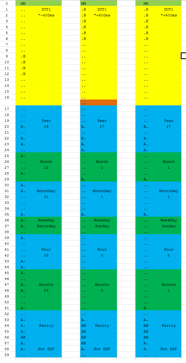
Here’s what happened in the minute before the leap second, the minute of the leap second and the minute following the leap second…

MM is the minute marker (500ms carrier off, 500ms carrier on), A and B show if the A or B bits are set.

MSF60_LeapSecond.png

Everything went nicely according to the MSF specification, the extra second was inserted at second +16.  The time signal gives the time that will prevail at the NEXT minute marker so we see the long minute encoding 00:00 1st Jan 2017 even though it was being transmitted towards the end of 2016.

For a leap second there is no indicator prior to its occurrence (not in MSF anyway, the clever DCF people have a leap second announcement at :19) so this all happens with a bit of a surprise however looking at the data it’s quite interesting to observe that given the leap second the DUT1 Code also has to change and change very significantly since time has just moved 1000ms.

DUT1 you say?  Never heard of it!  https://en.wikipedia.org/wiki/DUT1

So the MSF implementation could probably benefit from a bit of an enhancement such that if you are processing the last minute of the year then expect a leap second and if you see DUT1 change then it most likely has happened.

Not a big deal since phase is quickly regained but interesting nevertheless.

Happy New Year!

Posted in Uncategorized | Leave a comment

Pragotron Slave Clock – Part 4 – Odd’s and Ends

Given that my clock driver is complete and seems to work quite nicely I think I will move on to other projects however if anyone else is considering building their own variant to drive a vintage clock then I’ll leave just a couple of extra notes:

The connections I used were as follows:

LCD Driver : RS Pin 9, Enable Pin 8, 4 bit Data on Pins 7,6,5&4.
Clock Module: Data in on Pin 2, Power control on Pin 3.
H-Bridge Control: Enable A5, Direction1 Pin 12 and Direction2 Pin 11
Buttons on pins A3, A2 and A1.

All these can be changed in software if required.

If your clock does not require alternate pulses to change polarity then you don’t need an H-Bridge, just drive the voltage you need using a single FET.  Beware however that the coil in the clock is inductive so a scrubber diode might be advisable.

My menu system is very simple: RUN, SET, TZDIF, MANUAL and VERSION.  The first button changes mode with a long press, the other two buttons are up and down.

The controller needs to be told the current state of the hands when first powered using the MANUAL setting and thereafter it remembers the hand position even during power failure by recording the current state in EEPROM.  I use a levelling technique to reduce wear on any one EEPROM location, simple and should last the lifetime of the device.

Finally, be aware that the polarity of the clock does matter!  A pulse of the positive polarity will have no effect if applied when a negative pulse is required and vice versa.  Easily sorted out by swapping if you find yourself appearing to be one minute out and unable to advance.

Have fun and keep those vintage clocks in their original form!

And a nice video of the smaller version of my clock being made… https://www.youtube.com/watch?v=0LhkTH0tN-E

Posted in Uncategorized | 5 Comments

Pragotron Slave Clock – Part 3 – Software

My previous experiments around decoding long wave radio time signals primarily involved using the UK’s time signal MSF60 (https://en.wikipedia.org/wiki/Time_from_NPL) previously known as the Rugby time signal. This transmission no longer originates from Rugby, it moved north to cumbria and seems to have reduced power during the move, combined with the fact the the 60kHz signal seems to be drowned out by RF interference from my computer equipment made me look at alternatives.

Whilst looking around I stumbled across some work by Udo Klein (https://blog.blinkenlight.net/experiments/dcf77/dcf77-library/). Udo recognised the fact that interference to these signals was a big problem and wrote a library that would effectively use some digital signal processing techniques to improve the receivers immunity to noise.  Clearly where the signal is drowned out by computer RF interference all bets will be off but in locations where there is mostly a good chance of reception the algorithm does allow much noise to be ignored and lead to time recovery.

I extended this library for MSF and Udo has since merged these changes into the repository so you can try it out for yourself and see how you get on.  The performance seems a lot better than just using averaging and copes well with transients of noise.  Be aware however that correct positioning and orientation of the radio clock module is still vital, you need to experiment and should get flashes around 1 or 2Hz, crazy flashing probably means you are picking up your computer RFI rather than the time signal.

I have a collection of MSF and DCF modules now, either would work but for this project I decided to go with the last one I had connected so I am receiving the time signal from DCF77 (https://en.wikipedia.org/wiki/DCF77).

It seems that summer time for DCF77 now occurs at the same time that UK time changes it’s daylight savings (EU good for standard harmonisation, not so good for uncontrolled migration, un-democratic super-state etc, bring on June 23rd!) so the clock simply has to maintain a fixed offset and the daylight savings should work OK.

Most of the hardwork is done by Udo’s library but the extra code and a copy of the DCF77 decoder is here (https://gitlab.com/NivagSwerdna/SlaveClockDriver).

And it works!

Posted in Uncategorized | Leave a comment

Pragotron Slave Clock – Part 2 – High level design

So with my clock sitting idle on the wall it is time to come up with a design that will send it periodic pulses, once per minute, with +24V and then -24V on alternate minutes…

I really want this to be pretty stand-alone and I don’t want to faff about with WiFi so that eliminates NTP, I do not want to be near a window so that eliminates GPS so that leaves me with either a free-running clock or radio frequency receiver.  My recent experiments with the MSF radio signal, which is really hard to receive around computer equipment in London, led me to DCF77 which has similar problems but has better signal strength.  The MSF signal moved further up north a few years back and the transmission power was also reduced during the move so surprisingly DCF seems to work better here.

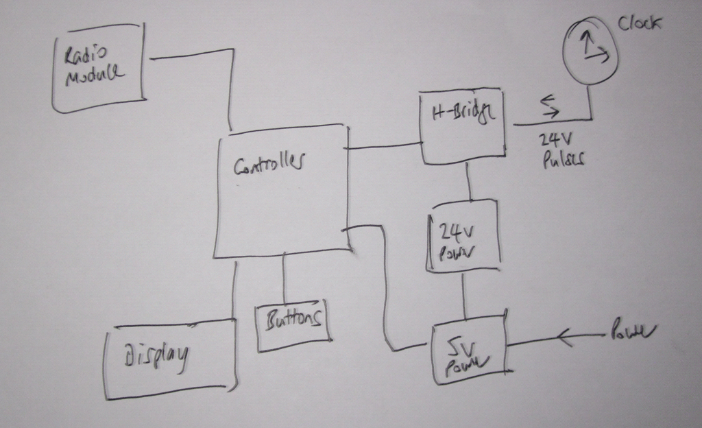
I plan to use some off-the-shelf parts so I’m not going to be clever in the first iteration at least… I need a controller, a radio clock module, a 24V supply, an H-bridge to send 24V (and reverse the direction each minute) and for fun an LCD display and a couple of buttons to change modes etc.  Modules are cheap as chips from China so I’m just going to attach a few things together and maybe later reduce the design and make a PCB.

block

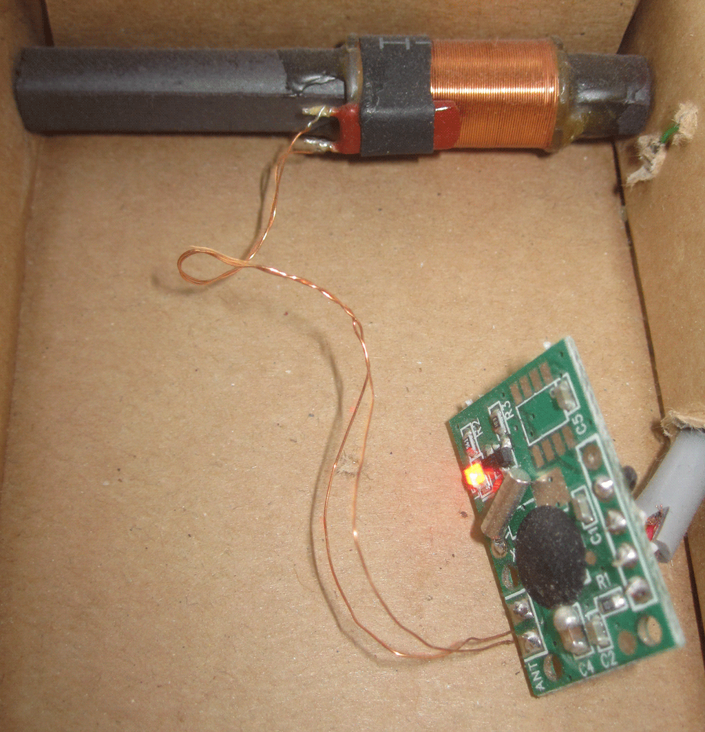
Here’s the Radio Module I bought from PV Electronics (http://www.pvelectronics.co.uk/index.php?main_page=product_info&cPath=9&products_id=8) (who also make nice NIXIE kits)…

DCF

I put it in a cardboard box for now, at the end of a bit of cable so I can move it away from my computer monitor.  RF Interference from computer equipment completely prevents reception using these receivers, the MSF 60kHz or 77kHz DCF signal being too close to the timebase in monitors etc.


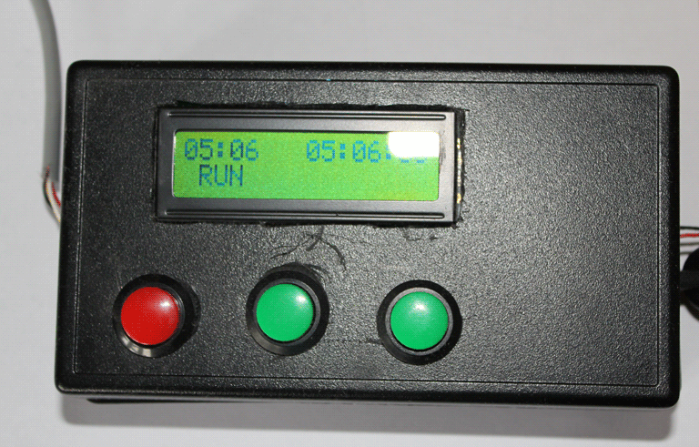
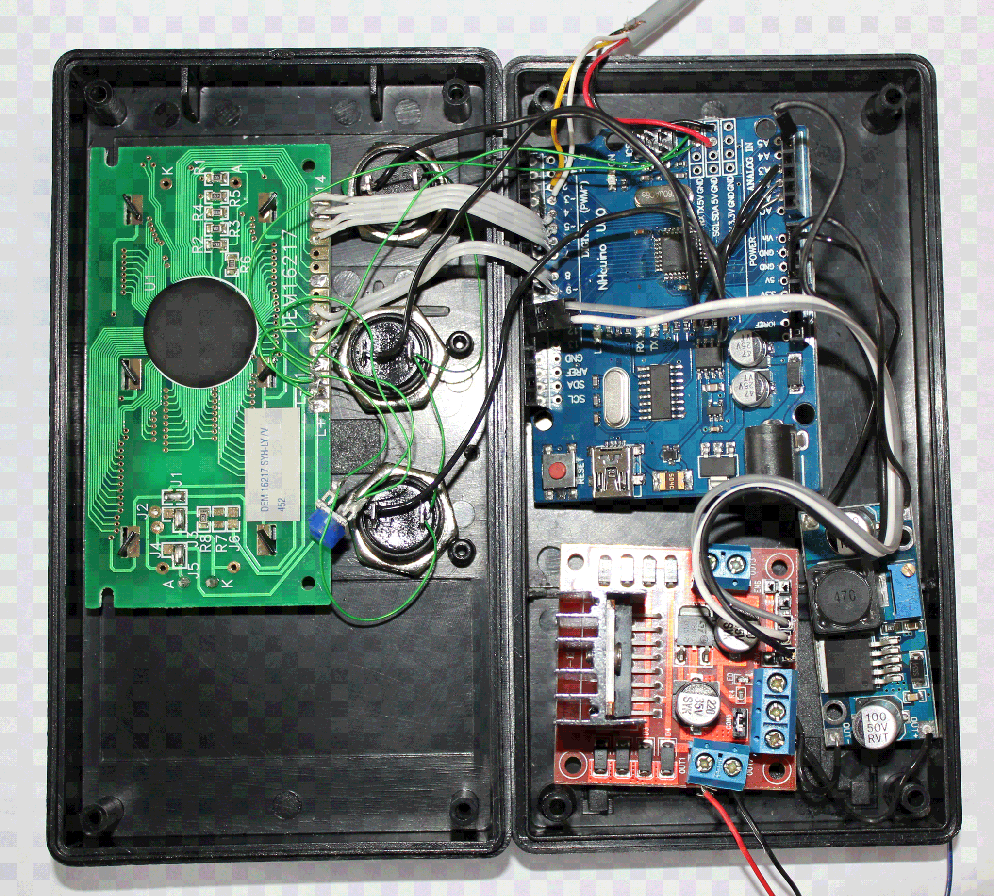
For the display I have a 16×2 LCD display with Hitachi controller in the junk box, for the controller a cheap chinese UNO clone and then a H-Bridge module and DC-DC converter (5V to 24V) from EBAY.  Three chunky buttons complete the hardware.

exterior

and inside the box…

Interior

The LCD display wires straight into the Arduino UNO, with just a small 10k potentiometer to allow the contrast to be varied, it is a 5V display so compatible with the 5V Uno clone. The DC-DC converter is just a quick and dirty way to turn 5V into 24V and the H-Bridge a simple (rather over the top way) of being able to reverse polarity to the clock.  (The radio module is located in the cardboard box for present a metre or so away).

It’s almost unbelievable how cheap some of these parts have become.  The L298N H-Bridge can be had for around £1.50 from HK on Ebay, the XL6009 DC-DC converter for around £1 and with a bit of shopping around the Uno clone is about £2.50.  So hardware cost is around £10 plus the radio module.

When choosing a Arduino Uno clone take time to try and find one with a crystal oscillator (shiny metal can next to processor) since the DCF decoding software needs a reasonably accurate local clock and some of the ceramic resonators in the Uno clones are terrible (2000 ppm).  If you are unlucky enough to get one with a ceramic resonator then with a bit of careful soldering you can easily replace the resonator with a crystal.

Posted in Uncategorized | Leave a comment